- 您现在的位置:买卖IC网 > Sheet目录1995 > DS4425BN+ (Maxim Integrated Products)IC OSC CLOCK 425MHZ 10-LCCC
DS4106/DS4212/DS4425
106.25MHz/212.5MHz/425MHz
Clock Oscillators
2
_______________________________________________________________________________________
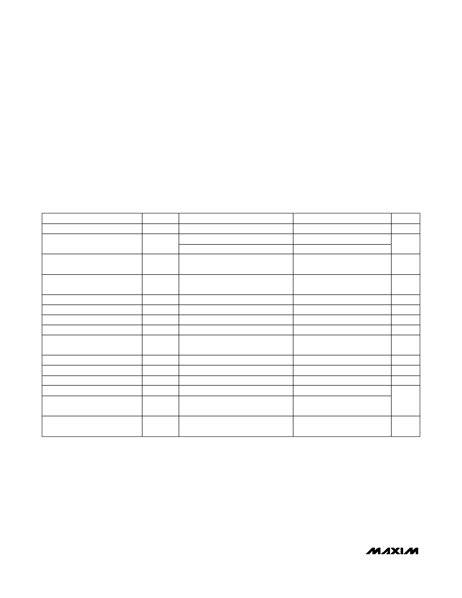
ELECTRICAL CHARACTERISTICS
(VCC = 3.0V to 3.6V, TA = -40°C to +85°C, typical values are at VCC = +3.3V and TA = +25°C, unless otherwise noted.) (Note 1)
Stresses beyond those listed under “Absolute Maximum Ratings” may cause permanent damage to the device. These are stress ratings only, and functional
operation of the device at these or any other conditions beyond those indicated in the operational sections of the specifications is not implied. Exposure to
absolute maximum rating conditions for extended periods may affect device reliability.
VCC, GND, OE, OUTP, OUTN .....................................-0.3V, +4V
Operating Temperature Range ...........................-40
°C to +85°C
Junction Temperature ......................................................+150
°C
Storage Temperature Range .............................-40
°C to +125°C
Soldering Temperature Profile
(3 passes max) ...............................See IPC/JEDEC J-STD-020
Specification
PARAMETER
SYMBOL
CONDITIONS
MIN
TYP
MAX
UNITS
Supply Voltage
VCC
(Note 2)
3.0
3.3
3.6
V
LVPECL (Note 3)
50
65
Supply Current
ICC
LVDS
53
67
mA
TTL Control Input-Voltage High
(OE)
VIH
(Note 2)
2
VCC
V
TTL Control Input-Voltage Low
(OE)
VIL
(Note 2)
0
0.8
V
Input Leakage Current
IIL
GND
OE
VCC
-50
+10
μA
LVPECL OUTPUTS (Note 4)
Output High Voltage
VOH
(Note 2)
VCC - 1.085
VCC - 0.88
V
Output Low Voltage
VOL
(Note 2)
VCC - 1.825
VCC - 1.62
V
Output Leakage Current
(Absolute)
IOL
OE = VIL
100
μA
LVDS OUTPUTS (Figure 2)
LVDS Output High Voltage
VOH
(Note 2)
1.475
V
LVDS Output Low Voltage
VOL
(Note 2)
0.925
V
LVDS Differential Output Voltage
|VOD|
250
400
LVDS Change in VOD for
Complementary States
|VOD|
25
mV
LVDS Offset Output Voltage
(Output Common-Mode Voltage)
VOS
(Note 5)
1.125
1.275
V
ABSOLUTE MAXIMUM RATINGS
发布紧急采购,3分钟左右您将得到回复。
相关PDF资料
DS4426T+T&R
IC DAC I2C-MARGINING 4CH 28-TQFN
DS4432U+
IC DAC 7BIT 2CH 5.5V 8-MSOP
DS4625P+150/200
IC OSC CLOCK 200MHZ 10-LCCC
DS4M133D+33
IC OSC CLOCK 133.33MHZ 10-LCCC
DS8005-RRX+
SMART CARD AFE DUAL 28SOIC
DSD1792DB
IC 24BIT STEREO AUD DAC 28-SSOP
EL5001IRE-T7
IC CLOCK DRIVER 6-CHAN 20-HTSSOP
FT10001L6X
IC RESET TIMER 6-MICROPAK
相关代理商/技术参数
DS4426
制造商:MAXIM 制造商全称:Maxim Integrated Products 功能描述:Quad-Channel, I2C-Margining IDACs with Three Channels of Power-Supply Tracking
DS4426T+
功能描述:数模转换器- DAC 4Ch I2C Migrt w/3 ch P-Sup Track RoHS:否 制造商:Texas Instruments 转换器数量:1 DAC 输出端数量:1 转换速率:2 MSPs 分辨率:16 bit 接口类型:QSPI, SPI, Serial (3-Wire, Microwire) 稳定时间:1 us 最大工作温度:+ 85 C 安装风格:SMD/SMT 封装 / 箱体:SOIC-14 封装:Tube
DS4426T+T&R
制造商:Maxim Integrated Products 功能描述: 制造商:Maxim Integrated Products 功能描述:28PIN 4X4 TQFN W/4 IDAC&3CH P/S TRA - Tape and Reel 制造商:Maxim Integrated Products 功能描述:IC DAC I2C-MARGINING 4CH 28-TQFN
DS4426T+T&R
功能描述:数模转换器- DAC 4Ch I2C Migrt w/3 ch P-Sup Track RoHS:否 制造商:Texas Instruments 转换器数量:1 DAC 输出端数量:1 转换速率:2 MSPs 分辨率:16 bit 接口类型:QSPI, SPI, Serial (3-Wire, Microwire) 稳定时间:1 us 最大工作温度:+ 85 C 安装风格:SMD/SMT 封装 / 箱体:SOIC-14 封装:Tube
DS4426T+TR
制造商:MAXIM 制造商全称:Maxim Integrated Products 功能描述:Quad-Channel, I2C-Margining IDACs with Three Channels of Power-Supply Tracking
DS443
制造商:未知厂家 制造商全称:未知厂家 功能描述:Analog IC
DS4432
制造商:MAXIM 制造商全称:Maxim Integrated Products 功能描述:Dual-Channel, I2C, 7-Bit Sink/Source Current DAC
DS4432U+
功能描述:数模转换器- DAC 2Ch I2C Adj Sink-Source RoHS:否 制造商:Texas Instruments 转换器数量:1 DAC 输出端数量:1 转换速率:2 MSPs 分辨率:16 bit 接口类型:QSPI, SPI, Serial (3-Wire, Microwire) 稳定时间:1 us 最大工作温度:+ 85 C 安装风格:SMD/SMT 封装 / 箱体:SOIC-14 封装:Tube